| Title | Size | Downloads |
|---|---|---|
| H3C AMD G6 Servers RAS Technology White Paper-6W101-book.pdf | 1.14 MB |
- Table of Contents
- Related Documents
-
| Title | Size | Download |
|---|---|---|
| book | 1.14 MB |
H3C AMD G6 Servers RAS
Technology White Paper
Copyright © 2024 New H3C Technologies Co., Ltd. All rights reserved.
No part of this manual may be reproduced or transmitted in any form or by any means without prior written consent of New H3C Technologies Co., Ltd.
Except for the trademarks of New H3C Technologies Co., Ltd., any trademarks that may be mentioned in this document are the property of their respective owners.
The information in this document is subject to change without notice.
Contents
Memory CE funnel and threshold mechanism
DRAM Error Check and Scrub (ECS)
DRAM Writeback Suppression on X4 Writes
DRAM Address/Command Parity with Replay
DRAM Write Data CRC with Replay
DRAM Read Data CRC with Replay
Decoding Last I/O Addresses Table
PCIe speed reduction and bandwidth reduction detection
PCIe Downstream Port Containment and Error Disconnect Recovery
PCIe Orderly and Surprise Hotplug
Automatic Boot-time DIMM MapOut
Automatic Boot-time Core Disable
PCIe® Advanced Error Reporting (AER)
CXL™ Component Error Reporting
ACPI Platform Error Interface (APEI)
APEI Boot Error Record Table (BERT)
APEI Hardware Error Status Table (HEST)
APEI Error Injection Table (EINJ)
DRAM Corrected Error Leaky Bucket Counters
DRAM Post-Package Repair (CPU)
MCA FruText and DIMM FRU Identification
IPMI command classification for RAS reporting
Overview
The server is one of the key components of any modern data center infrastructure. It includes various components such as processors, storage devices, PCIe devices, power supplies, and fans. To ensure service continuity, correct server operation based on data integrity are critical to a modern data center. In other words, we must avoid data corruption no matter data is stored in any server component (memory, cache, or processor registers) or transmitted through any platform links (xGMI or PCI Express).
When a server component fails, the set of reliability, availability and serviceability (RAS) features can meet the above requirements by maximizing service availability and maintaining data integrity.
Table 1 RAS definition based on H3C G6 servers
|
Item |
Definition |
|
Reliability |
Probability that the system produces the correct output within a given time T, as measured by the mean time between failures (MTBF) metric. It can be enhanced by avoiding, detecting, and repairing hardware failures. A reliable system does not provide incorrect data and calculation results, but can detect and correct data corruption. |
|
Availability |
Probability of correct system running at a given time, and the percentage of the actual running time of the server to the actual running time. |
|
Serviceability |
How easy and fast the system can be repaired or maintained. If the time for the system to repair errors increases, the serviceability decreases. Serviceability can be improved by simplifying system issue diagnosis and providing clear and intelligent advance warnings of failures to avoid system failures. |
Classify errors from high to low error severity into uncorrectable errors, delayed errors, correctable errors and transparent errors.
Table 2 Error categories
|
Item |
Definition |
|
Uncorrectable errors |
Errors that cannot be corrected by hardware are reported to software through Machine Check Exception (MCE). |
|
Delayed errors |
Errors that cannot be corrected by hardware but does not result in immediate interruption of program progress, loss of data integrity, or corruption of processor state. Delayed errors indicate that the data is poisoned but not used, such as poisoned data. |
|
Correctable errors |
Correctable errors can be fixed by hardware and do not lead to data loss or processor status damage. |
|
Transparent errors |
Errors that has been corrected by the hardware, does not result in data loss or processor state corruption, and the hardware is capable of correcting the next error in the same device. For example, a single-bit error occurs in a cache with double-bit error correction capability. |
Benefits
RAS can provide the following benefits:
· Increased system uptime—Increases system reliability for the system to stay longer, as measured by the Mean Time Between Failures (MTBF), Annual Crash Rate (ACR), or Annual Service Rate (ASR) metric.
· Reduced the duration of unexpected downtime—Adopts AMD EPYC processors to support synchronized hardware and firmware logging, helping users to identify and isolate errors and take preventive or proactive maintenance measures. This enables quick system restoration, reduces the cost of repairs, and mitigates the consequences of the outage to the business.
Outages are inevitable even with the best plans and processes. When an unplanned outage happens, a maintainable system can come back online quickly, as measure by the Mean Repair Time (MTTR) matric.
· Enhanced data integrity—RAS provides several mechanisms to prevent data corruption or correct poisoned data, which ensures data corruption can get contained once detected.
Applicable products
This document is applicable to the following H3C UniServer servers:
· H3C UniServer R3950 G6
· H3C UniServer R4950 G6
· H3C UniServer R5350 G6
· H3C UniServer R5500 G6 AMD
Using this document
The information in this document is subject to change over time.
The information in this document might differ from your product if it contains custom configuration options or features.
RAS system architecture
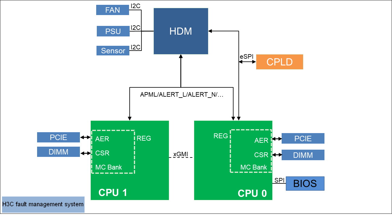
Based on AMD RAS architecture, H3C provides a complete fault management system together with hardware, the BIOS, HDM, and OS error processing mechanisms. The system can provide functions such as error diagnosis, error location, error correction, information collection, and error reporting. Since the core of the system runs on the BIOS and HDM, it does not rely on the OS and can perform all-time detection of the system and take corresponding measures once an error occurs.
As shown in Figure 1, the fault management system contains the hardware layer, CPLD, processor platform, HDM (out-of-band management), the BIOS, and OS.
· HDM—Core of the error location system. It is responsible for error information collection and analysis and can display error information as event logs or alarms from the Web interface.
· Processor platform—Supported by AMD EPYC processors, which provides more powerful management of errors occurred on processors, memory modules, and PCIe devices.
· CPLD—Connects downlink hardware modules, including power supplies, fans, and other underlying hardware (except processors, memory modules, drives, and standard PCIe modules), captures hardware exceptions, connects to HDM at the uplink, and transmits error information.
· BIOS—Collects and locates errors occurred on processors, memory modules, PCIe devices, and storage devices, provides error location results to HDM, and provides OS-level error management interfaces, such as APEI, to the OS.
· Web interface—Web interface provided by management tools, such as HDM, for users to maintain the server locally or remotely. Users can use the Web interface together with LEDs of specific server components to manage the server.
· Involved protocols—Protocols used by the fault management system includes eSPI, SPI, PCIe, UART, I2C, SMBUS, and LocalBus.
Figure 1 H3C fault management system architecture
RAS operating mechanism
The basic error processing schemes of RAS are as follows:
· For transparent errors, no further action is required at the upper layers, as the hardware has already corrected the errors.
· For correctable errors, RAS marks the error location and fast repair the corresponding module. Users will not aware the occurrence of such errors.
· For delayed errors, the location of toxic data will be immediately marked, and by limiting the spread of poisoned data, delayed errors will be prevented from evolving into more serious problems.
· For uncorrectable errors, RAS isolates the errors by isolating bad memory blocks or degrading the bus to maintain system operation. If severe errors occur and result in system outage, you must use HDM to restore or restart the system.
RAS technology for AMD G6 servers is realized based on the following mechanisms:
· Maintain reliable operation through robust components and maximum error detection.
· Avoid system failures by reducing global errors, error correction, and continuing operation despite uncorrectable errors.
· Avoid system downtime (mainly for planned downtime) through the following methods:
¡ First-time error diagnosis: Try to capture enough data to complete the error diagnosis when the mistake occurs for the first time.
¡ Internal redundancy design and online maintenance capabilities: Allows for continuous operation without replacing parts or problem-solving without shutting down. For more information about redundancy design and online maintenance, see the detailed introduction.
· Flexibility: The choice of whether to enable a function is primarily implemented in the firmware, not in the hardware.
The new and improved RAS features in the AMD Genoa/G6 are as follows:
· Reliability improvement:
¡ Support Advanced Memory Device Correction (AMDC).
¡ Support DRAM Error Check and Scrub (ECS).
¡ Support DRAM read and write data CRC.
¡ Support PCIe/CXL LCRC + replay.
¡ Support PCIe/CXL.io ECRC.
¡ Support PCIe/CXL.io uncorrected error detection.
· Availability improvement:
¡ Support on-chip watchdog timers.
¡ Support PCIe system firmware intermediary.
· Maintainability improvement (diagnosis and repair):
¡ Support in-band error reporting.
¡ Support memory error reporting.
¡ Support out-of-band error monitoring.
¡ Support DRAM runtime post-package repair.
¡ Support error injection.
¡ Support error injection on secure silicon.
· Added features:
¡ DRAM Corrected Error Leaky Bucket Counters.
¡ Advanced Platform Management Link interface (APML).
Figure 2 RAS schemes
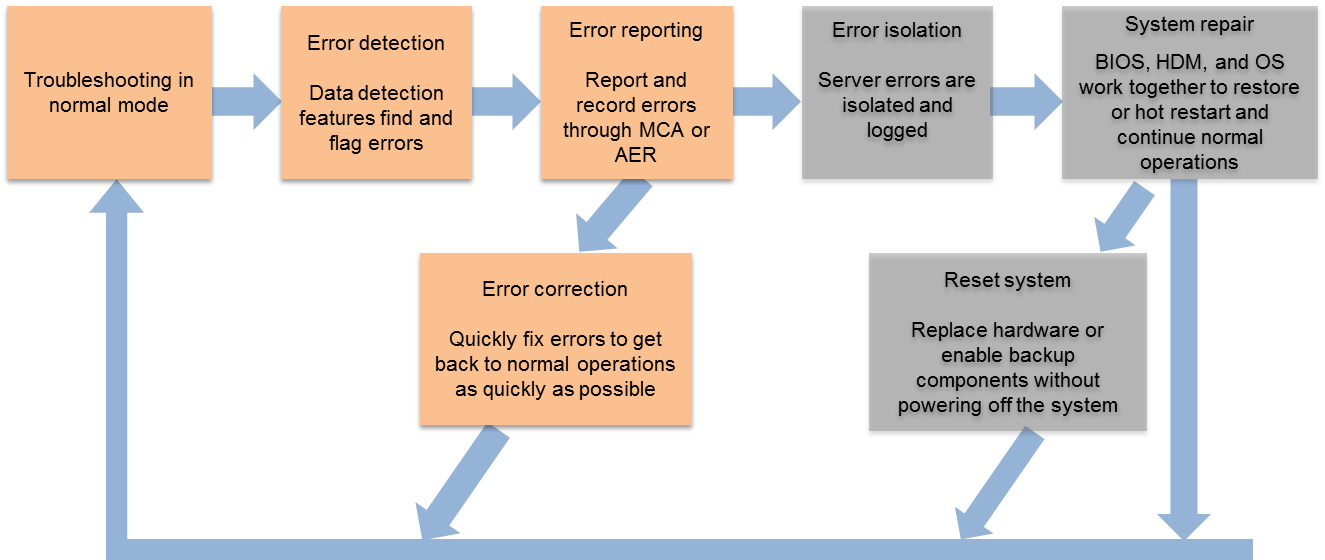
The following introduces the key points of AMD RAS technology according to the processes of error detection, reporting, and processing.
Error detection
Error detection of AMD G6 series servers is mainly achieved through ECC, Parity and CRC technologies in key components and areas. Errors are mainly divided into data errors, bus errors and logical function errors. The corresponding common methods of error detection are as follows:
· The general data module uses ECC and Parity for detection.
· The bus interface module uses the CRC for detection.
· The logic functional module uses the Timeout for detection.
Error correction is generally achieved through ECC and Retry. The main data and bus module's error detection and error correcting capability are shown in Table 3.
Table 3 Error detection methods for different modules
|
Module |
Detection method |
|
CPU Core |
Parity |
|
L1 Data Cache |
ECC |
|
L1 Data Tag |
ECC |
|
L1 Instruction TLB |
Parity + Retry |
|
L1 Instruction Cache |
Parity + Retry |
|
L1 Instruction Tag |
Parity + Retry |
|
L2/L3 Cache |
DEC-TED ECC |
|
L2/L3 Cache Tag |
SEC-DED ECC |
|
DRAM Address/Command |
Parity + Replay |
|
DRAM Write Data |
CRC + Replay |
|
Memory Controller |
SEC-DED ECC |
|
Memory Controller DF |
Parity |
|
NBIO, PCIE and NBIF |
Parity + ECC |
|
SATA |
Parity |
|
USB |
ECC |
|
FCH A-Link |
Parity |
|
On-Chip Data Bus |
Parity |
|
Off-Package Link Packet |
Parity + Retry |
|
On-package and off-package PHY Controller |
ECC |
|
System Probe Filter |
ECC |
|
System Management Network |
Parity |
|
SMN Off-Package Link Packet |
CRC + Retry |
|
SMN On-Package Link Packet |
CRC + Retry |
|
SMU |
Parity + ECC |
|
MP5 |
Parity + ECC |
|
PSP |
Parity + ECC |
|
Parameter Block |
ECC |
The most error-prone part of the CPU is the data storage module in the CPU, that is, the cache at all Layers. The AMD G6 server series offers comprehensive cache protection mechanisms, including ECC for Layer 1 data cache, parity check for Layer 1 instruction cache, and double-error correction, triple error detection (DEC-TED) for Layer 2 and Layer 3 cache. Compared to traditional single-error correction and double error detection (SEC-DED) ECC, it adds an additional correction layer. EC-TED reduces the impact of multi-bit transient errors by correcting double-bit errors and also reduces the impact of single-bit hard faults. EC-TED is able to correct a second single-bit error in the affected part of the cache.
In addition to ECC, the memory also supports Patrol Scrubber, Redirect Scrubber and Poison Scrubber. Some memory locations might not be accessed for a long time. The Patrol Scrubber's periodic memory inspection function periodically traverses all memory zones, correcting correctable mistakes. It's a good, low-cost method for checking memory and enhancing data integrity. Redirect Scrubber refers to the operation of correcting the error and writing the correct data back to the memory if a correctable error is found when the CPU instruction actively reads the memory data. The AMD G6 series server also supports Poison Scrubber, which marks the location of poison data to prevent reporting unnecessary delay errors.
Error reporting
The system reports detected errors and generates error log messages. The AMD G6 series server supports four types of error reporting methods: MCA, MCAX, AER, and AMPL.
MCA records processor and system hardware errors for reporting to the operating system. When an error is detected, MCA will save information about the error in specific registers and interrupt error reporting of the specified type. For hardware correctable errors, the software logs error information for subsequent diagnosis and repair. If the error cannot be corrected, the error is classified as an uncorrectable error. When an uncorrectable error occurs, the system immediately takes steps to correct the error and resume the interrupted program. If the error cannot be corrected by software, MCA determines the extent of the impact of the uncorrected error on the execution instruction flow and the architectural state of the processor or system, and then takes action to control the impact of the failure by terminating the damaged software process.
For errors that are not corrected and have no direct impact on the system, processor kernel, or the schema state of any currently executing thread, the hardware (HW) may classify them as delayed errors. Information about latency errors will be logged but not reported via MCE. Instead, the hardware continuously monitors for errors and upgrades them to uncorrectable errors when an error condition is about to affect the execution of the instruction flow or cause corruption of the processor core or system architectural state. At this point, if the reporting for this mistake source is enabled, it will trigger a disrupt in MCE to report the error. If the error can be corrected at the system level, it may be possible to restore the affected programs. If the error cannot be corrected, the operating system can terminate the affected program without shutting down the entire system.
The processor also supports Machine Check Architecture Extensions (MCAX), which is AMD's x86-64 expansion of MCA. It provides a richer MCA bank than traditional MCA and provides bank ownership all the way to a single kernel. Since each bank is owned by a single kernel, the MCA register can only be accessed from the MCA main thread, which helps ensure that interrupts from the machine checking the bank are routed to the appropriate thread. The MCA X architecture supports up to 256 MCA groups, each with 16 memory registers. The expanded MCA architecture holds more information about system health, which can be queried to speed troubleshooting.
Advanced Error Reporting (AER) is mainly used to report and handle PCIe errors. AER can locate the error source in the PCIe architecture, provides a standardized control mechanism for error messages received by PCIe Root through interrupt reporting, and can distinguish the severity of various uncorrectable errors.
Advanced Platform Management Link (APML) follows the SMBus protocol, also known as Sideband Interface (SBI). APML provides an interface for out-of-band access to MCA registers. You can use the APML interface to communicate with the server's out-of-band management system HDM so that error information can be directly obtained by HDM
Error processing
If a mistake is detected but cannot be corrected, the impact of the error is minimized through data poisoning marking or fault tolerance on the link.
Data poisoning is a mechanism that enables machine check recovery by transforming global uncorrected errors into local uncorrected errors, reducing the frequency of system interrupts. Data poisoning involves detecting, marking, and tracing uncorrectable data errors. As poisoned data moves through the system, the poisoned state is retained in memory, cache, and links so that the poisoned data is not used by the system. When marked by data poisoning, uncorrectable data errors can lead to fatal conditions for the system. Through data poisoning, uncorrectable data errors can be contained within the process context. When the system terminates the affected process, other processes and the system itself are not affected. The system remains available despite data errors. When the CPU attempts to use data marked as poison, poisoning consumption occurs. The poisoning consumption passes the Machine Check Anomaly (MCE) in the context of the consumption process or task, enabling the MCA to identify the process consuming data and proceed with restoration or termination. When the processor detects poisoned data, it logs a delayed error in the MCA bank to identify the location of the uncorrectable data error, helping determine if hardware failure has occurred and reconfigure the system to prevent the use of faulty hardware.
In terms of memory, AMD G6 series servers support the JEDEC-defined Post Package Repair (PPR) feature, which supports configuring spare DRAM rows to replace faulty ones. The combination of hardware and firmware support from the processor enables both soft (reconfigurable) and hard (permanent) repair, ensuring that DIMMs with problematic DRAM rows can be reconfigured and maintain the same level of reliability as before the issue occurred.
In terms of PCIe, the PCIe bus is protected by AER and EDPC, which can help isolate and recover from errors on the PCIe link. When an uncorrectable error occurs on a PCIe root port, the EDPC feature can recover by disconnecting and reconnecting the affected PCIe link. To ensure uninterrupted operation of devices under the OS, the PCIe root port saves the context of the PCIe endpoint device before disconnecting the link. After the link is restored, the context information of the PCIe endpoint is accurately recovered to ensure the system operates unaffected.
Memory CE funnel and threshold mechanism
Memory CE funnel mechanism
The memory CE funnel mechanism is designed to manage and control Correctable Error (CE) events on the AMD G6 platform. By reducing the value by one within a set time and discarding the value, memory CE funnel controls the frequency of overall error event reporting. The AMD Genoa platform provides the following features:
· Funnel enablement register: Used to enable or disable the funnel feature. The disabling state is equivalent to the faucet being closed in Figure 3.
· Speed register: Used to set the flow rate, which is equivalent to the degree to which the faucet is opened or closed as shown in Figure 3.
Figure 3 Memory CE funnel mechanism

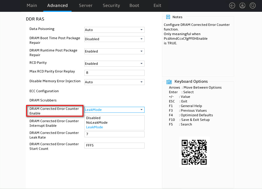
Selecting the LeakMode or NoLeakMode mode
Set the DRAM Corrected Error Counter Enable value from the BIOS Setup Utility. Options include:
· LeakMode—Enable the funnel feature.
· NoLeakMode—Disable the funnel feature.
Figure 4 Selecting the LeakMode or NoLeakMode mode
Setting the Leak Rate
Set the DRAM Corrected Error Counter Leak Rate value from the BIOS Setup Utility.
Figure 5 Setting the Leak Rate
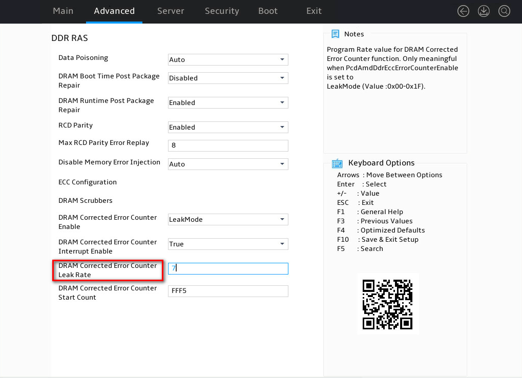
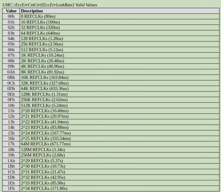
Figure 6 shows available values of the leak rate. The default value is 07h, which represents leak one memory CE every 10.24 us.
Based on experience, it is generally recommended to discard one CE per second. Therefore, you can select the closest available option, which is 18h, meaning one is discarded every 1.34 seconds.
Figure 6 Available values of the leak rate
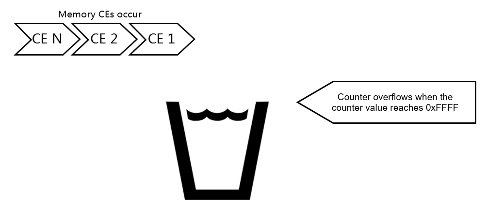
Memory CE threshold
The memory CEs are accumulated by a counter. The counter starts at the Start Count value and increases by 1 every time a CE occurs. When the counter value reaches 0xFFFF, the counter overflows, which triggers an SMI interrupt. The BIOS starts to execute the interrupt.
Figure 7 Memory CE threshold
Setting the Start Count for the memory CE counter
Set the DRAM Corrected Error Counter Start Count value from the BIOS Setup Utility to specify the start value of the counter.
Figure 8 Setting the Start Count value for the memory CE counter
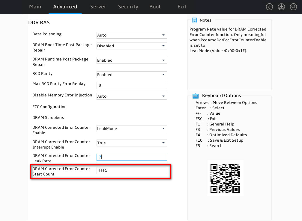
When the counter value reaches 0xFFFF, it triggers an SMI interrupt. The BIOS starts to execute the interrupt.
From this, it can be determined that the memory CE threshold is the value between Start Count and 0xFFFF. The threshold is calculated as follows:
For example, if the target threshold is 5000:
Start Count = 0xFFFF – 5000 = 0xEC77
Therefore, set the BIOS Setup option value to 0xEC77.
Setting the Memory CE Report Count Threshold
You can choose to report errors based on the frequency of persistent memory CEs. When the set threshold is met, SMI interrupts are masked to prevent memory CE reporting, enhancing system reliability and accuracy.
The default value of the Memory CE Report Count Threshold option on the BIOS Setup Utility is 1.
SMI interrupt control
Setting the MCA error threshold
You can set the threshold for correctable errors in the Machine Check Architecture (MCA). When the count reaches 0xFFF, it will trigger an SMI interrupt.
Configuring SMI storm suppression
To prevent performance impacts from excessive SMI interrupts, the AMD platform offers an SMI storm suppression mechanism. When Machine Check Exception (MCE) frequency exceeds 5 times per second, the system enters SMI Polling mode, handling MCE events at a rate of 5 times per second. Once the frequency drops below 5 times per second, the system reverts to SMI Interrupt mode.
Memory CE report method
Memory CE reporting to BMC
The BIOS reports memory CE information through the IPMI interface, which includes three formats: SEL log, SDS log, and OEM IPMI commands.
Memory CE reporting to OS
The BIOS reports error records to the ACPI Table using APEI-HEST-GHES. You can view these records in the OS using the dmesg command.
Reliability
Memory RAS
On-chip ECC/Parity
|
Feature name |
On-chip ECC/Parity |
|
Description |
The processor protects critical on-chip SRAM, triggers, and latch arrays using ECC or parity check. The array can prevent multi-bit errors through interleaving. |
|
Purpose |
Improve system reliability and accuracy. |
|
Configuration |
Disabled by default and can be enabled from the BIOS. |
|
Remarks |
N/A |
DRAM ECC
|
Feature name |
DRAM ECC |
|
Description |
The memory controller of the processor supports two different error correction codes. Both DRAM error correction codes use symbol-based coding to form ECC. x4 ECC uses 36 4-bit symbols to generate a 144-bit ECC containing 128 data bits and 16 parity bits. x16 ECC uses 18 16-bit symbols to generate a 288-bit ECC containing 256 data bits and 32 parity bits. When x4 DRAM devices are used on an 80-bit channel, x16 ECC with Advanced Memory Device Correction (AMDC) can correct all errors caused by a single failed DRAM device. x16 ECC is compatible with the DDR5 limited-failure specification, providing better correction performance when using x8 DRAM devices on an 80-bit channel or x4 DRAM devices on a 72-bit channel. |
|
Purpose |
Improve system reliability and accuracy. |
|
Configuration |
Enabled by default and can be configured from the BIOS. |
|
Remarks |
N/A |
DRAM Error Check and Scrub (ECS)
|
Feature name |
DRAM Error Check and Scrub (ECS) |
|
Description |
The memory controller periodically corrects single-bit errors detected by ECC within the chip. This feature must be enabled in the memory controller. When a DRAM device exceeds a specific error threshold, the MCA of the memory controller records the error channel, device, bank, and row. |
|
Purpose |
Improve system reliability and accuracy. |
|
Configuration |
Enabled by default and can be configured from the BIOS. |
|
Remarks |
N/A |
DRAM Writeback Suppression on X4 Writes
|
Feature name |
DRAM Writeback Suppression on X4 Writes |
|
Description |
DRAM provides a method to suppress data write-back during a read-modify-write (RMW) operation when writing to X4. |
|
Purpose |
X4 device error correction write-back inhibition. |
|
Configuration |
Disabled by default and can be configured from the BIOS. |
|
Remarks |
N/A |
DRAM UECC Retry
|
Feature name |
DRAM UECC Retry |
|
Description |
If an uncorrected ECC error occurs, the processor can retry the command, providing recovery for transient errors on the data bus. If retrying doesn't result in an ECC error or corrects it, data is forwarded and the corrected error is recorded. If the maximum retry count is reached and the uncorrected ECC error persists, the data is poisoned, and the delayed error is recorded. |
|
Purpose |
Improve system reliability and accuracy. |
|
Configuration |
Disabled by default and can be configured from the BIOS. |
|
Remarks |
N/A |
DRAM Address/Command Parity with Replay
|
Feature name |
DRAM Address/Command Parity with Replay |
|
Description |
Based on the JEDEC DDR5 standard, the processor implements RCD parity check on the DDR5 address or command bus. If a parity check error occurs, the command can be replayed. This feature provides detection and recovery for transient errors on the bus. |
|
Purpose |
Improve system reliability and accuracy. |
|
Configuration |
Enabled by default and can be configured from the BIOS. |
|
Remarks |
N/A |
DRAM Write Data CRC with Replay
|
Feature name |
DRAM Write Data CRC with Replay |
|
Description |
According to the JEDEC DDR5 standard, the processor performs cyclic redundancy check (CRC) on the write data packets. If a CRC error occurs, the command can be replayed. This function provides detection and recovery for transient errors on the bus. |
|
Purpose |
Improve system reliability and accuracy. |
|
Configuration |
Disabled by default and can be configured from the BIOS. |
|
Remarks |
N/A |
DRAM Read Data CRC with Replay
|
Feature name |
DRAM Read Data CRC with Replay |
|
Description |
According to the JEDEC DDR5 standard, the processor performs cyclic redundancy check (CRC) on the read data packets. If a CRC error occurs, the command can be replayed. This function provides detection and recovery for transient errors on the bus. Errors not corrected through replay will result in data poisoning and record delayed errors. |
|
Purpose |
Improve system reliability and accuracy. |
|
Configuration |
Disabled by default and can be configured from the BIOS. |
|
Remarks |
N/A |
DRAM Patrol Scrubber
|
Feature name |
DRAM Patrol Scrubber |
|
Description |
DRAM performs read-modify-write operations periodically on memory locations to detect and correct potential errors. This feature is awakened once per cycle and checks the next sequential position in memory. The processor can configure this feature to simultaneously erase multiple address ranges, improving erase speed on systems with high memory occupancy. |
|
Purpose |
Improve system reliability and accuracy. |
|
Configuration |
Enabled by default and can be configured from the BIOS. |
|
Remarks |
N/A |
DRAM Redirect Scrubber
|
Feature name |
DRAM Patrol Scrubber |
|
Description |
When a read request encounters a correctable ECC error, the DRAM redirect handling feature will be invoked as necessary. This feature immediately writes the corrected data back to memory. |
|
Purpose |
Improve system reliability and accuracy. |
|
Configuration |
Enabled by default and can be configured from the BIOS. |
|
Remarks |
N/A |
GMI/xGMI RAS
On-Package Link Errors
|
Feature name |
On-Package Link Errors |
|
Description |
CRC errors might occur in the GMI/xGMI encapsulation. When correctable CRC errors exceed a threshold, they are recorded in MCA to indicate system performance degradation. Uncorrectable errors in the link will also be logged in MCA, resulting in a system fatal error event. |
|
Purpose |
Improve the reliability of GMI/xGMI link data transmission. |
|
Configuration |
Enabled by default and can be configured from the BIOS. |
|
Remarks |
N/A |
Off-Package Link Errors
|
Feature name |
Off-Package Link Errors |
|
Description |
The external GMI/xGMI link encapsulation might encounter CRC errors. When correctable CRC errors exceed a threshold, they are recorded in MCA to indicate system performance degradation. Uncorrectable errors in the link will also be logged in MCA, resulting in a system fatal error event. |
|
Purpose |
Improve the reliability of GMI/xGMI link data transmission. |
|
Configuration |
Enabled by default and can be configured from the BIOS. |
|
Remarks |
N/A |
PCIe RAS
PCIe® End-to-End CRC
|
Feature name |
PCIe® End-to-End CRC |
|
Description |
The processor supports generating PCIe ECRC and checking all PCIe root ports. For peer-to-peer requests passing through the processor, ECRC is not preserved. Typically, ECRC generation should only be enabled in the root ports and endpoints when there are switches between them. |
|
Purpose |
Achieve higher data integrity when exchanging data between two PCIe endpoints. |
|
Configuration |
Enabled by default. |
|
Remarks |
N/A |
Availability
Data Poisoning
|
Feature name |
Data Poisoning |
|
Description |
When a system encounters a poison, it will attempt to mark it. The marking process generates poison consumption, which in turn results in reporting to the MCA during the consumption process in the context. |
|
Purpose |
Improve system reliability. |
|
Configuration |
Automatically takes effect and cannot be disabled. |
|
Remarks |
N/A |
Fatal Error Recovery
|
Feature name |
Fatal Error Recovery |
|
Description |
When the CPU detects an unmarked, unrecoverable error, it acts to contain data corruption, issuing a system-level fatal error event to the internal Data Fabric module. This event freezes the Data Fabric's data transmission queues to prevent bad data propagation to non-volatile storage. In the event of a system fatal error, the CPU supports system recovery through a warm reset and the option for an out-of-band MCA information collection in case of a system hang during the warm reset. If warm reset fails, the CPU initiates a cold restart, also supporting the triggering of a system hang before the cold restart. To facilitate debugging, the processor logs all fatal error events in the NBIO MCA bank. AMD recommends platforms to shield fatal errors in the NBIO MCA, as fatal errors will still be recorded in the original block's MCA (or MCAX). |
|
Purpose |
Improve system reliability. |
|
Configuration |
The Reset after Sync-Flood menu controls whether a hot reset is executed when a fatal error occurs. When this menu is set to TRUE, a fatal error triggers a hot reset. When set to FALSE, a fatal error will not trigger a hot reset. |
|
Remarks |
N/A |
Machine Overflow Recovery
|
Feature name |
Machine Overflow Recovery |
|
Description |
Machine Overflow Recovery allows system recovery in overflow situations. When MCi_STATUS[Overflow] records a non-fatal error, Machine Overflow Recovery is supported. If a system-critical error occurs, Machine Overflow Recovery is not allowed. When Machine Overflow Recovery is supported, software records all system critical situations via MCA_STATUS[PCC]. If Machine Overflow Recovery is not supported, unrecoverable errors recorded in MCA_STATUS[Overflow] will not be logged as recovery errors. |
|
Purpose |
Improve system reliability. |
|
Configuration |
Automatically takes effect and cannot be disabled. |
|
Remarks |
N/A |
CPU Watchdog Timers
|
Feature name |
CPU Watchdog Timers |
|
Description |
The CPU watchdog timer (WDT) is used to detect situations where the x86 kernel cannot make forward progress and to recover from them. It is a configurable counter that is reset upon completion of each instruction operation. If no operation is completed within a specified time, a system fatal error event is generated. |
|
Purpose |
Use a watchdog timer to track execution progress and detect when the processor is unable to continue forward execution. |
|
Configuration |
Enabled by default. |
|
Remarks |
N/A |
Decoding Last I/O Addresses Table
|
Feature name |
Decoding Last I/O Addresses Table |
|
Description |
When a fatal error occurs, diagnostic software records the Last I/O address to DF::OrigWdtAddrLogLo and DF::OrigWdtAddrLogHi. The address range 0 to FFFFFFFC_FFFFFFFF corresponds to DRAM or MMIO, and the specific physical DRAM location can be determined further through the OS's memmap. The range FFFFF_10000000 to FFFFF_1FFFFFF corresponds to a PCIe device, where bits 27-20 represent the bus, bits 19-15 represent the device, and bits 14-12 represent the function, allowing identification of the specific PCIe device location. The range FFFFFFD_FC000000 to FFFFFFD_FC00FFFF corresponds to PCIe I/O. |
|
Purpose |
Identify whether the fatal error is caused by an external component through the decoded address. |
|
Configuration |
Enabled by default and collected through ADDC. |
|
Remarks |
N/A |
DRAM Thermal Throttling
|
Feature name |
DRAM Thermal Throttling |
|
Description |
When approaching DIMM temperature limits, the processor supports thermal throttling. It increases refresh rates to maintain data integrity and imposes bandwidth limits on the command bus. The processor also supports firmware-driven bandwidth limits, enabling a response to platform-detected events using APML. |
|
Purpose |
Increase availability by avoiding downtime situations due to exceeding temperature limits. |
|
Configuration |
Enabled by default and can be configured from the BIOS. |
|
Remarks |
N/A |
CPU Thermal Throttling
|
Feature name |
CPU Thermal Throttling |
|
Description |
The processor supports thermal throttling when approaching temperature limits. Increase availability by avoiding downtime situations due to exceeding temperature limits. |
|
Purpose |
Improve system availability and maintainability. |
|
Configuration |
Enabled by default and partially configurable. |
|
Remarks |
N/A |
PCIe speed reduction and bandwidth reduction detection
|
Feature name |
PCIe speed reduction and bandwidth reduction detection |
|
Description |
The processor supports thermal throttling when approaching temperature limits. Increase availability by avoiding downtime situations due to exceeding temperature limits. |
|
Purpose |
Improve system availability and maintainability. |
|
Configuration |
Enabled by default and partially configurable. |
|
Remarks |
N/A |
PCIe Downstream Port Containment and Error Disconnect Recovery
|
Feature name |
PCIe Downstream Port Containment and Error Disconnect Recovery |
|
Description |
The processor supports the DPC functionality described in the PCIe specification, including RP PIO extension and DL_Active ERR_COR signal. Platform firmware and operating systems coordinate using downstream port containment (DPC) and Surprise Down functionality of the processor to support PCIe link error recovery. |
|
Purpose |
Avoid propagation of potentially bad data with error isolation and recovery on PCIe links |
|
Configuration |
Enabled by default and can be configured from the BIOS. |
|
Remarks |
N/A |
PCIe Orderly and Surprise Hotplug
|
Feature name |
PCIe Orderly and Surprise Hotplug |
|
Description |
Supports hot-swapping of PCIe devices, allowing users to replace faulty devices and restore the server to normal operation when the system is not powered on. |
|
Purpose |
Improve system availability. |
|
Configuration |
Enabled by default and can be configured from the BIOS. |
|
Remarks |
N/A |
DRAM Memory Tester
|
Feature name |
DRAM Memory Tester |
|
Description |
The processor offers the capability to test installed memory to check for damaged DIMMs. During the reset sequence, the memory tester writes and reads data to a set of addresses on each installed channel and DIMM in the system. If an uncorrectable ECC error is detected while accessing a DIMM, it is marked as damaged. When a DIMM is marked as damaged, the processor disables it and performs a system hot reset to reinitialize the memory mapping without the DIMM in the system. |
|
Purpose |
The memory tester's purpose is not to exhaustively search for all DIMM errors, but to test for completely damaged DIMMs. |
|
Configuration |
Enabled by default. |
|
Remarks |
N/A |
Automatic Boot-time DIMM MapOut
|
Feature name |
Automatic Boot-time DIMM MapOut |
|
Description |
If one of the two memory tests, PMU training and Agesa Memory Test, fails, the failed memory will be moved out of the Map and disabled. |
|
Purpose |
Improve system memory reliability and stability. |
|
Configuration |
Enabled by default. |
|
Remarks |
N/A |
Automatic Boot-time Core Disable
|
Feature name |
Automatic Boot-time Core Disable |
|
Description |
This processor implements a feature where if the core fails the Built-In Self-Test (BIST), it can be ignored from the active configuration. If a core or cache fails the BIST, the processor will report the faulty core complex and attempt to boot with the minimum number of core complexes as specified in the processor programming reference. |
|
Purpose |
Automatically disable cores that have not passed the Built-In Self-Test. |
|
Configuration |
Disabled by default. |
|
Remarks |
N/A |
Serviceability
In-band Error Reporting
Machine Check Architecture
|
Feature name |
Legacy x86 Machine Check Architecture (MCA) |
|
Description |
The processor implements the x86 Machine Check Architecture (MCA). MCA defines a way to record processor and system hardware errors and report them to system software, allowing system software to play a role in the recovery and diagnosis of hardware errors. |
|
Purpose |
Ensure component-level reliability. |
|
Configuration |
Automatically takes effect and cannot be disabled. |
|
Remarks |
N/A |
|
Feature name |
AMD Machine CheckArchitecture Extensions(MCAX) |
|
Description |
MCAX, an extension of the Machine Check Architecture, provides a richer feature set than the traditional x86 Machine Check Architecture. The extended features include: · Expansion of MCA banks: Supports extending the number of MCA banks supported by AMD processors to support comprehensive error logging for many blocks in the processor. · Expansion of MCA banks size: Enhanced error handling, improved diagnostics, and finer configuration by recording extended information in MCA Banks. · Single-kernel ownership of MCA banks: Each MCA register set is only visible to one core, and no software synchronization is required when accessing MCA set registers. |
|
Purpose |
Enhance BIOS control over faults. |
|
Configuration |
Automatically takes effect and cannot be disabled. |
|
Remarks |
N/A |
|
Feature name |
Machine Check Architecture (MCA) Thresholding |
|
Description |
The error threshold is used to count the number of errors, and the processor implements the x86 MCA threshold through the MCA_MISCx register. Supports setting error threshold via saturation counter, SMI interrupt will be sent on overflow. |
|
Purpose |
Enhance BIOS fault control. |
|
Configuration |
Enabled by default and can be configured from the BIOS. |
|
Remarks |
N/A |
Platform First Error Handling
|
Feature name |
Platform First Error Handling (PFEH) |
|
Description |
The processor implements platform-first error handling, enabling all errors logged in the MCA to be reported first to the platform firmware rather than to the operating system or hypervisor. This feature allows the platform firmware to take platform-specific action (for example, repair or log) for each error before notifying the operating system or hypervisor. For example, platform firmware can implement predictive failure analysis to reduce service costs or future downtime. |
|
Purpose |
Enhance BIOS fault control. |
|
Configuration |
Enabled by default and can be configured from the BIOS. |
|
Remarks |
N/A |
PCIe® Advanced Error Reporting (AER)
|
Feature name |
PCIe AER |
|
Description |
Each PCIe root port on the processor supports AER, enabling advanced error handling, diagnostics and recovery capabilities for PCIe devices. This feature works on physical root ports that connect external devices and internal root ports that connect internal PCIe devices. The processor supports OS-first and firmware-first reporting of PCIe AER errors. |
|
Purpose |
Enhance BIOS fault control. |
|
Configuration |
Enabled by default and can be configured from the BIOS. |
|
Remarks |
N/A |
CXL™ Error Handling
|
Feature name |
CXL Error Handling |
|
Description |
The processor supports CXL protocol version 1.1. For CXL support, the processor provides up to 4 RCs per Package, and each RC supports up to 4 CXL ports. That is, each Package supports up to 16 CXL memory devices. CXL error handling mainly includes device error handling and protocol layer error handling. |
|
Purpose |
Enhance BIOS fault control. |
|
Configuration |
Enabled by default and can be configured from the BIOS. |
|
Remarks |
N/A |
CXL™ Protocol Error Reporting
|
Feature name |
CXL Protocol Error Reporting |
|
Description |
CXL protocol fault reporting is completed by the PCIe AER register and the CXL Ras capability structure. Therefore, the strategy used to control CXL protocol fault reporting will be affected by the PCIe AER control strategy. If CXL protocol fault reporting is set to firmware priority, then CXL protocol fault reporting follows the firmware priority principle. If CXL protocol fault reporting is set to PCIe AER reporting, then CXL protocol error reporting follows the PCIe AER fault reporting policy. |
|
Purpose |
Enhance BIOS fault control. |
|
Configuration |
Enabled by default and can be configured from the BIOS. |
|
Remarks |
N/A |
CXL™ Component Error Reporting
|
Feature name |
CXL Component Error Handling |
|
Description |
CXL component faults are reported by CXL devices that support the Mailbox interface defined by the CXL Memory device register. For firmware-first fault reporting, each CXL device component that supports CXL component failures provides GHES/CPER structures for fault reporting in the system. |
|
Purpose |
Enhance BIOS fault control. |
|
Configuration |
Enabled by default and can be configured from the BIOS. |
|
Remarks |
N/A |
PMIC Error Handling
|
Feature name |
PMIC Error Handling |
|
Description |
On DDR5, the PMIC provides voltage to the DDR core/IO and VPP. According to the JEDEC PMIC specification, PMIC can report faults. The ability of PMIC fault recovery depends on different PMIC manufacturer strategies. In the memory initialization phase, the PMIC register is read to collect fault information. In the firmware execution phase, PMIC faults are reported to BMC and recorded in the BERT table. |
|
Purpose |
Enhance BIOS fault control. |
|
Configuration |
Enabled by default and can be configured from the BIOS. |
|
Remarks |
N/A |
Machine Check Alert
|
Feature name |
Machine Check Alert |
|
Description |
When an MCA error occurs, the CPU sends an alert to APML. The CPU will record this alert in the SB-RMI RasStatus register, which can be accessed through APML. |
|
Purpose |
Enhance BIOS fault control. |
|
Configuration |
Enabled by default. |
|
Remarks |
N/A |
Fatal Error Alert
|
Feature name |
Fatal Error Alert |
|
Description |
When a fatal error occurs, the CPU sends an alert to APML. The CPU will record this alert in the SB-RMI RasStatus register, which can be accessed through APML. At the same time, when a fatal error occurs, the CPU also supports disabling the hot reset action, which can be used to enable MCA collection after a fatal error occurs. |
|
Purpose |
Enhance BIOS fault control. |
|
Configuration |
Enabled by default. |
|
Remarks |
N/A |
Thermal Throttle Alert
|
Feature name |
Thermal Throttle Alert |
|
Description |
The processor supports thermal throttling event alerts. SB-TSI has high/low thresholds that trigger the ALERT_L signal to the BMC. |
|
Purpose |
Enhance BIOS fault control. |
|
Configuration |
Enabled by default. |
|
Remarks |
N/A |
MCA Mailbox
|
Feature name |
MCA Mailbox |
|
Description |
The processor supports two BMC Mailbox commands for querying and retrieving any valid MCA: BMC_RAS_MCA_VALIDITY_CHECK and BMC_RAS_MCA_MSR_DUMP. If warm restart response to fatal errors is disabled, these Mailbox commands can be used at runtime or after a fatal error is generated. |
|
Purpose |
Enhance BIOS fault control. |
|
Configuration |
Enabled by default. |
|
Remarks |
N/A |
Legacy SB-RMI MCA Interface
|
Feature name |
Legacy SB-RMI MCA Interface |
|
Description |
The processor supports the Legacy SB-RMI MCA interface for polling MCA registers. Accessing MCA state through SB-RMI or MSR in-band modes does not conflict. In the event of a severe error, MCA registers cannot be accessed before a reset. As a best practice, use the MCA mailbox method to access MCA instead of this Legacy interface. |
|
Purpose |
Enhance BIOS fault control. |
|
Configuration |
Enabled by default. |
|
Remarks |
N/A |
Reset Reason Mailbox
|
Feature name |
Reset Reason Mailbox |
|
Description |
FCH provides a register that holds the reason for previous restarts. The S5_Reset_Status register of the FCH contains the cause of the last reset, including hardware-induced fatal errors, x86 triple-fault shutdown events, and push-button and software-triggered resets. |
|
Purpose |
Enhance BIOS fault control. |
|
Configuration |
Enabled by default. |
|
Remarks |
N/A |
ACPI Platform Error Interface (APEI)
|
Feature name |
APEI |
|
Description |
Supports industry-standard Advanced Configuration and Power Interface Platform Error Interface (APEI) version 6.2. AMD supports the Hardware Error Status Table (HEST), Boot Error Recording Table (BERT), and Error Injection Table (EINJ). |
|
Purpose |
Improve system availability and maintainability. |
|
Configuration |
Enabled by default and cannot be configured. |
|
Remarks |
N/A |
APEI Boot Error Record Table (BERT)
|
Feature name |
|
|
Description |
All errors logged at startup create an entry in BERT and are divided into general error data entries, memory error entries, memory parity error entries, PCIe error entries and processor error entries according to the error type. |
|
Purpose |
Record startup errors and report them to the operating system. |
|
Configuration |
Enabled by default. |
|
Remarks |
N/A |
APEI Hardware Error Status Table (HEST)
|
Feature name |
APEI Hardware Error Status Table (HEST) |
|
Description |
Supports the ACPI standard HEST table to define hardware-related error sources and error types. Errors reported via standard MCA, MCAX support MCE error sources, CMCI sources and DMC sources (MCAX) or PFEH interfaces. |
|
Purpose |
Implementation of standardized software and hardware error interfaces. |
|
Configuration |
Enabled by default. |
|
Remarks |
N/A |
APEI Error Injection Table (EINJ)
|
Feature name |
APEI Error Injection Table (EINJ) |
|
Description |
AMD supports error injection for type 3, 4, and 5 errors through APEI's EINJ table. The firmware allows separate injection and triggering of each error type. · Type 3 error injection injects correctable DRAM ECC errors at the specified address. · Type 4 error injection injects uncorrectable DRAM ECC errors at the specified address, to be reported and recorded as deferred errors. · Type 5 error injection injects uncorrectable DRAM ECC errors at specified addresses. The triggering action of a Type 5 injection causes the operating system to read the error location and log and report a delay error, and an uncorrectable poison consumption error to be logged and reported via MCA. |
|
Purpose |
Support memory ECC error injection and verify related functions. |
|
Configuration |
Enabled by default. |
|
Remarks |
N/A |
Out of Band Error Monitoring
|
Feature name |
Out of Band Error Monitoring |
|
Description |
The processor supports out-of-band error monitoring through the APML interface. This can be used by a BMC or similar functional entity to monitor errors occurring on the CPU. |
|
Purpose |
Enhance system control over failures. |
|
Configuration |
Enabled by default. |
|
Remarks |
N/A |
DRAM Corrected Error Leaky Bucket Counters
|
Feature name |
|
|
Description |
The processor provides a 16-bit DRAM correction error counter for each chip select, which is incremented when a corrected ECC error is detected. For DIMMs that support column multiplication, the memory controller provides a counter for each column multiplier per chip select. When the counter is saturated, an SMI or APIC-based LVT interrupt can optionally be generated. |
|
Purpose |
Improves memory reliability and reduces the likelihood of data corruption or system crashes. |
|
Configuration |
Enabled by default. |
|
Remarks |
N/A |
Boot Status Indicators
|
Feature name |
Boot Status Indicators |
|
Description |
Boot Status Indicators indicate the status of the boot process. If issues occur during boot, the indicators pinpoint the problem, enabling fault detection. |
|
Purpose |
Improved system availability and maintainability. |
|
Configuration |
Enabled by default. |
|
Remarks |
N/A |
DRAM Post-Package Repair (CPU)
|
Feature name |
|
|
Description |
The JEDEC-defined post-package repair (PPR) feature allows a spare DRAM row to be configured to replace a faulty or failed row. The processor provides hardware and firmware support, allowing soft (reconfigurable) and hard (permanent) fixes. |
|
Purpose |
Using DDR5 DRAM PPR, DIMMs with problematic DRAM rows can be reconfigured and maintain the same level of reliability as before the problem occurred. |
|
Configuration |
Enabled by default. |
|
Remarks |
N/A |
MCA Address Translation
|
Feature name |
MCA Address Translation |
|
Description |
When a DRAM ECC error occurs, the Ecc error address recorded by the memory controller in the MCA register is a truncated version (relative to the normalized address). The truncated version address needs to be converted into the system physical address through a specific interface before it can be used directly by the platform firmware or operating system. Similarly, the truncated version address needs to be converted into a DRAM physical address through a specific interface before it can be directly used by the platform firmware to obtain DRAM chip select/row/bank/column and other information. |
|
Purpose |
Used to report and record DRAM Ecc errors. |
|
Configuration |
The DXE stage uses AMD_RAS_SERVICE_DXE_PROTOCOL to perform MCA Address conversion. The Rumtime stage uses AMD_RAS_SERVICE_SMM_PROTOCOL to perform MCA Address conversion. |
|
Remarks |
The platform firmware aligns the translation with the provided interface before performing any processing on the DRAM Address recorded in the MCA register. |
MCA FruText and DIMM FRU Identification
|
Feature name |
MCA FruText and DIMM FRU Identification |
|
Description |
The memory controller records the characteristic information of each Error in the MCA_SYND1_UMC and MCA_SYND2_UMC registers. The CPU supports filling some platform-related FruText information in the MCA error log reported to the operating system into these MCA_SYND1_UMC and MCA_SYND2_UMC registers. MCA FruTestju encoding example: Perr Sx:Txx:Bxx: · Perr—Processor Error · S—Socket# · T—Thread# · B—Bank# · x—hexadecimal number For example, Perr S0:T0a:B1f. |
|
Purpose |
Used to quickly analyze the meaning of MCA Error. |
|
Configuration |
Set PcdAmdMcaFruTextEnable to not TRUE. |
|
Remarks |
· For platform firmware: ¡ The platform firmware needs to implement the DIMM FRU recognition Protocol (DXE_RAS_OEM_DIMMMAP_PROTOCOL) to provide the platform-related memory map table. ¡ The platform firmware needs to populate the FruText field values into HEST and BERT tables. · For operating system (Linux): ¡ When MCA_CONFIG[FruTextInSynd] is 1, print MCA_SYND1 and MCA_SYND2 as ASCII characters in the MCA error log. ¡ When MCA_CONFIG[FruTextInSynd] is 0, print MCA_SYND1 and MCA_SYND2 as hexadecimal numbers in the MCA error log. |
Platform RAS features
ABL RAS
|
Feature name |
ABL RAS |
|
Description |
During the ABL stage, the processor performs a series of error detection and reporting processes, including: · Executing memory initialization. · Performing DDR training and recording training results. · Conducting MBIST testing and recording test results. · Collecting MBIST data in APOB and storing it in memory. · The driver retrieves MBIST results and DDR training results. · Transmitting error information through Error Codes. |
|
Purpose |
Implement error detection and reporting during the ABL stage. |
|
Configuration |
Enabled by default and can be configured from BIOS. |
|
Remarks |
N/A |
Error Injection
|
Feature name |
ABL RAS |
|
Description |
To assist with software testing and debugging, the processor supports hardware interfaces for fault injection. Supported error types for injection include: · On-chip ECC/parity check (NBIO, SMU/PSP/MPIO, UMC, and PCIe). · DRAM ECC. · DRAM UECC retry. · DRAM address/command parity check and replay. · On-Package Link Errors. · Off-Package Link Errors. · PCIe LCRC. · PCIe End-to-End CRC. · USB ECC. · SATA parity check. |
|
Purpose |
Convenient for server testing and debugging. |
|
Configuration |
Enabled by default. |
|
Remarks |
N/A |
IPMI command classification for RAS reporting
|
index |
Error Types |
NETFUN |
BMC_LUN |
CMD |
SubCmd |
Description |
Reporting Stage |
|
1 |
McaErr |
0x36 |
0x00 |
0x2a |
0x03 |
Report MCAerr register Runtime stage POST stage |
DXE, SMM |
|
2 |
MemTestErr |
0x36 |
0x00 |
0x2a |
0x06 |
Report MemTestErr POST stage |
DXE |
|
3 |
PcieErr |
0x36 |
0x00 |
0x2a |
0x04 |
Report PcieErr Runtime stage POST stage |
DXE, SMM |
|
4 |
SmnErr |
0x36 |
0x00 |
0x2a |
0x05 |
Report SmnErr POST stage |
DXE |
|
5 |
NbioErr (Not Implemented) |
|
|
|
|
|
|
|
6 |
ReportAbsentMemTestErrToBMC (Absent dimm) |
0x36 |
0x00 |
0x2a |
0x08 |
POST stage |
DXE |
|
7 |
PMIC Error |
0x36 |
0x00 |
0x2a |
0x09 |
POST stage |
DXE |
|
8 |
SATA Error (Not Implemented) |
|
|
|
|
|
|
|
9 |
USB Error (Not Implemented) |
|
|
|
|
|
|
|
10 |
NbioSyncFloodFromPin |
0x36 |
0x00 |
0x2a |
0x0a |
POST stage. |
DXE |
|
11 |
DRAM ECC Error |
0x36 |
0x00 |
0x2a |
0x0b |
Runtime stage. |
SMM |
|
12 |
McaErr threshold |
0x36 |
0x00 |
0x04 |
0x39 |
Report the MCA CPU err register Runtime stage |
SMM |
|
13 |
PCIeErr threshold |
0x36 |
0x00 |
0x04 |
0x3a |
Report PCIe err aer register Runtime stage |
SMM |
SMI storm suppression
|
Feature name |
SMI storm suppression |
|
Description |
AMD supports SMI Polling storm suppression. When the CE error reaches the threshold, the SMI interrupt is triggered to report the error. When the triggered SMI reaches the threshold within a certain period of time, an SMI storm is considered to have occurred, and the Polling Mode is entered for suppression, and SMI interrupts are no longer triggered. |
|
Purpose |
When an SMI storm occurs, suppress it to avoid system downtime. |
|
Configuration |
RAS Periodic SMI Control is enabled by default. |
|
Remarks |
N/A |
SWITCH RAS
|
Feature name |
SWITCH RAS |
|
Description |
SWITCH also has slot numbers and can note and report errors like ordinary PCIe devices. |
|
Purpose |
SWITCH can normally trigger RAS related mechanisms. |
|
Configuration |
Consistent with ordinary PCIe devices. |
|
Remarks |
N/A |
